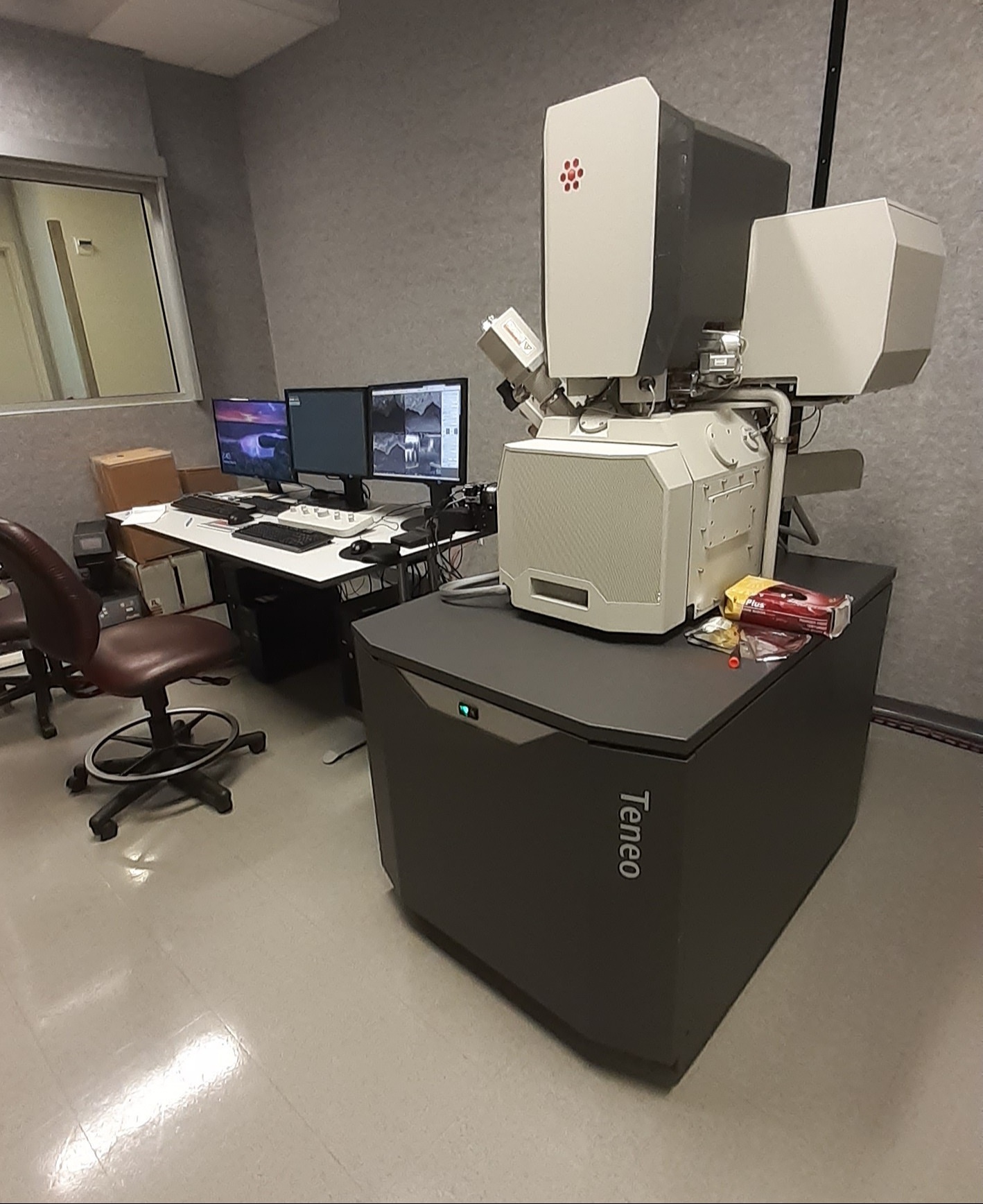
The FEI TeneoTM is an ultra-high-resolution analytical Scanning Electron Microscope that delivers outstanding performance for a broad range of challenging samples, including magnetic and non-conducting materials. The in-lens FEI Trinity™ detectors collect all signals simultaneously, saving time and offering distinctly different contrasts to capture the maximum amount of data.
Imaging and Analytical Modes
- High Vacuum, high resolution with the automated Optiplan mode
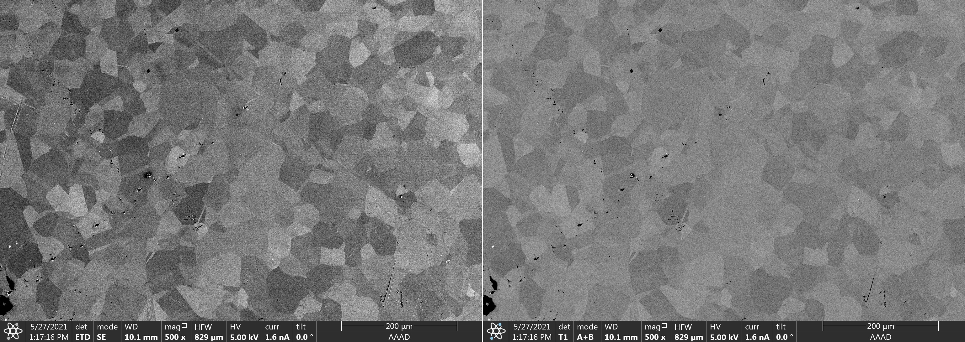
The two in-lens (T1, T2) and one in-column (T3) detectors allow simultaneous collection of secondary and backscatter electrons from 1 pA to 400 nA beam current and 200 eV to 30 keV beam energy - Grain/crystal orientation contrast imaging on highly polished materials at low incident beam energy
- Energy Dispersive Spectroscopy (EDS) using EDAX Octane Elite SDD
This system includes detectors with a silicon nitride (Si3N4) window, offering remarkable improvements in low energy sensitivity for light element detection and low kV microanalysis.- 125 eV resolution at Mn Ka at 10k cps
- Carbon detection above 750k input cps for ultra-fast mapping and particle acquisition
- Detection range: Al L (73 eV) to Am
- Crystal Orientation Imaging Microscopy via Velocity Super EBSD Camera
The Velocity™ Super Electron Backscatter Diffraction (EBSD) Camera
offers high-speed EBSD mapping with the highest indexing performance
on real-world materials. Powered by a CMOS sensor, the Velocity
combines fast acquisition with high sensitivity and low noise performance
for optimal collection and data quality.- Data collection rates up to 4,500 indexed points/second allowing EBSD mapping within minutes
- High-speed, low-noise CMOS sensor allows high accuracy indexing at fast speed
- Orientation precision ofless than 0.1°
- High-speed simultaneous EDS-EBSD collection
Uses and Applications
- High-resolution imaging ~20 nm resolution for conductive and non-conductive materials without the need of coating
- Better Z-contrast imaging up to as low as 200 eV beam energy and 20 eV landing energy
- Surface sensitive high resolution imaging
- Elemental mapping and semi-quantitative compositional analysis using energy dispersive spectroscopy (EDS)
- Grain analysis (grain size, orientation and texture) using electron backscatter diffraction (EBSD)

| HOURLY RATES | ||
| Users | Daytime | Overnight M-F: 5pm - 8am Sat-Sun: All Day |
| On-Campus | $45.00 | $22.50 |
| Off-Campus Academic | $69.30 | $34.65 |
| Industry | $90.00 | $45.00 |
CONTACT US FOR RESERVATIONS:
| Dr. Paulo Perez | Lab: 801-587-3108 Office: 801-581-6855 |
Images, Elemental Maps, Crystal Orientation Collected from the TENEO System

BSE images of a lithium-ion battery cathode acquired simultaneously by the T2 (high angle, left), T1 (medium angle, middle), and ETD (low angle, right) detectors. Sample courtesy of T. Kazda, Brno University of Technology. Images copied from ThermoScientific White paper on Trinity Detection System (authors: Petr Wandrol, EJR Vesseur, Radovan Vasina, Alex Ilitchev).

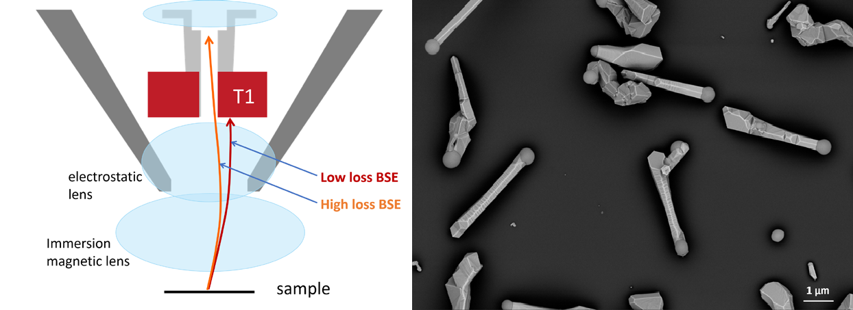
(Left) Diagram of BSE energy filtering with the compound final lens. (Right) T1 low-loss BSE image of self-catalyzed GaAs nanowires on Si (111) substrate. Sample courtesy of David Fuster, Andrés Raya, Álvaro San Paulo and María Ujue González of the IMM-Instituto de Microelectrónica de Madrid (CNM-CSIC). Images copied from ThermoScientific White paper on Trinity Detection System (authors: Petr Wandrol, EJR Vesseur, Radovan Vasina, Alex Ilitchev)

(Left) SE and (Right) BSE images showing grain contrast on highly polished Ni with the use of low-energy incident beam

(Left) Spectra acquired from a chromium nitride sample at 10 kV. Comparing the scaled spectra to the Cr K peak clearly shows the increased nitrogen and oxygen peak intensities achieved with a Si3N4 window. (Right) Al L to Al K peak height ratio of 1:1 at 2.5 kV. Images copied from Ametek spec sheet for Octane Elite System.

(A) EBSD orientation map from additively manufactured Inconel 718 was collected at 4,500. indexed points per second at 25 nA beam current. (B) EBSD orientation map from Inconel 600 was collected at 3,000 indexed points per second at 11 nA beam current with >99% indexing success. (C) EBSD orientation map of deformed ferritic steel was collected at ≈ 2,500 indexed points per second. (D) EBSD orientation map of additively manufactured titanium (HCP + BCC phases) was collected at ≈2,500 indexed points per second. Images copied from Ametek spec sheet for Velocity Super EBSD Camera System.