| HOURLY RATES | ||
| Users | Daytime | Overnight M-F: 5pm - 8am Sat-Sun: All Day |
| On-Campus | $45.00 | $22.50 |
| Off-Campus Academic | $69.30 | $34.65 |
| Industry | $90.00 | $45.00 |
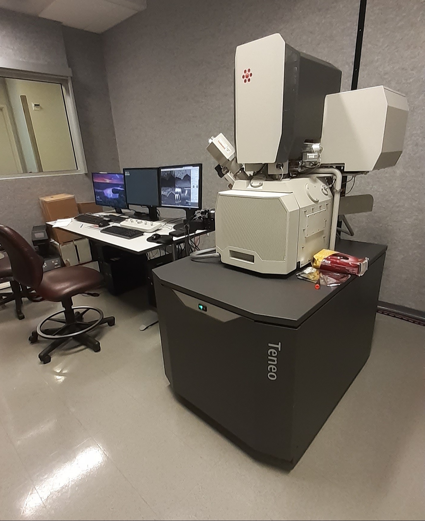
CONTACT US FOR RESERVATIONS:
| Dr. Paulo Perez | Lab: 801-587-3108 Office: 801-581-6855 |
, T1 (medium angle, middle), and ETD (low angle, right) detectors. Sample courtesy of T. Kazda, Brno University of Technology. Images copied from ThermoScientific White paper on Trinity Detection System (authors: Petr Wandrol, EJR Vesseur, Radovan Vasina, Alex Ilitchev).</p>")
BSE images of a lithium-ion battery cathode acquired simultaneously by the T2 (high angle, left), T1 (medium angle, middle), and ETD (low angle, right) detectors. Sample courtesy of T. Kazda, Brno University of Technology. Images copied from ThermoScientific White paper on Trinity Detection System (authors: Petr Wandrol, EJR Vesseur, Radovan Vasina, Alex Ilitchev).
 Diagram of BSE energy filtering with the compound final lens. (Right) T1 low-loss BSE image of self-catalyzed GaAs nanowires on Si (111) substrate. Sample courtesy of David Fuster, Andrés Raya, Álvaro San Paulo and María Ujue González of the IMM-Instituto de Microelectrónica de Madrid (CNM-CSIC). Images copied from ThermoScientific White paper on Trinity Detection System (authors: Petr Wandrol, EJR Vesseur, Radovan Vasina, Alex Ilitchev) </p>")
(Left) Diagram of BSE energy filtering with the compound final lens. (Right) T1 low-loss BSE image of self-catalyzed GaAs nanowires on Si (111) substrate. Sample courtesy of David Fuster, Andrés Raya, Álvaro San Paulo and María Ujue González of the IMM-Instituto de Microelectrónica de Madrid (CNM-CSIC). Images copied from ThermoScientific White paper on Trinity Detection System (authors: Petr Wandrol, EJR Vesseur, Radovan Vasina, Alex Ilitchev)
 SE and (Right) BSE images showing grain contrast on highly polished Ni with the use of low-energy incident beam</p>")
(Left) SE and (Right) BSE images showing grain contrast on highly polished Ni with the use of low-energy incident beam
 Spectra acquired from a chromium nitride sample at 10 kV. Comparing the scaled spectra to the Cr K peak clearly shows the increased nitrogen and oxygen peak intensities achieved with a Si<sub>3</sub>N<sub>4</sub> window. (Right) Al L to Al K peak height ratio of 1:1 at 2.5 kV. Images copied from Ametek spec sheet for Octane Elite System.</p>")
(Left) Spectra acquired from a chromium nitride sample at 10 kV. Comparing the scaled spectra to the Cr K peak clearly shows the increased nitrogen and oxygen peak intensities achieved with a Si3N4 window. (Right) Al L to Al K peak height ratio of 1:1 at 2.5 kV. Images copied from Ametek spec sheet for Octane Elite System.
</strong> EBSD orientation map from additively manufactured Inconel 718 was collected at 4,500. indexed points per second at 25 nA beam current. <strong>(B)</strong> EBSD orientation map from Inconel 600 was collected at 3,000 indexed points per second at 11 nA beam current with >99% indexing success. <strong>(C)</strong> EBSD orientation map of deformed ferritic steel was collected at ≈ 2,500 indexed points per second. <strong>(D)</strong> EBSD orientation map of additively manufactured titanium (HCP + BCC phases) was collected at ≈2,500 indexed points per second. Images copied from Ametek spec sheet for Velocity Super EBSD Camera System.</p>")
(A) EBSD orientation map from additively manufactured Inconel 718 was collected at 4,500. indexed points per second at 25 nA beam current. (B) EBSD orientation map from Inconel 600 was collected at 3,000 indexed points per second at 11 nA beam current with >99% indexing success. (C) EBSD orientation map of deformed ferritic steel was collected at ≈ 2,500 indexed points per second. (D) EBSD orientation map of additively manufactured titanium (HCP + BCC phases) was collected at ≈2,500 indexed points per second. Images copied from Ametek spec sheet for Velocity Super EBSD Camera System.