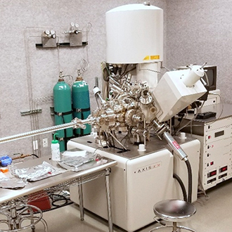
X-RAY, AUGER, ULTRAVIOLET PHOTOELECTRON SPECTROSCOPY (XPS),(AES),(UPS): KRATOS AXIS ULTRA
- Quantitative chemical analysis of the top 10 nm surface layer
- Identification of bonding and oxidation state of elements on the surface
- Overlayer thickness measurement up to ~10 nm
- Depth profiling of up to ~100 nm using Ar+ ion sputtering
- Fermi-level and work function measurement via ultraviolet photoelectron spectroscopy (UPS) with He(I) and He(II) sources
- Scanning electron and scanning auger microscopy ~15 μm resolution
- Chemical analysis of the top monolayer using ion scattering spectroscopy (ISS) with He ion source
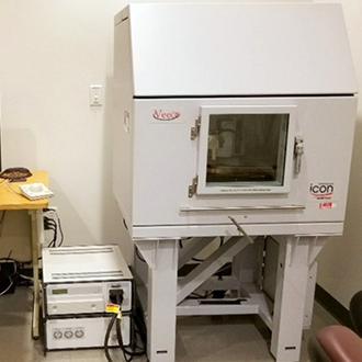
ATOMIC FORCE MICROSCOPY (AFM): Bruker Icon
- High-resolution imaging and measurement of surface height features at angstrom scales
- Quantitative measurement of sub-nanometer scale surface roughness
- Easy instrument operation with the use of Bruker ScanAsyst™ and PeakForce™ tapping modes
- Contact and tapping imaging modes
- Magnetic force microscopy
- Fluid cell imaging for biological samples
- Special deep trench probe for high aspect ratio surface features
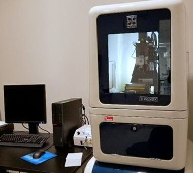
NANOINDENTER: Bruker Hysitron TI Premier
- Measurement of material hardness, Young’s modulus, fracture toughness and other mechanical properties
- Analysis of semiconductors, polymers, metals, thin films, and multiple layers
- Identication of topographical features
- Acquire additional information about the deformation in post-scanning, and measure quantitative RMS surface roughness
- Maximum applicable load ~100 μN
- Nanoscale mechanical and tribological behavior of materials at elevated temperatures up to 800°C
- Optional inert gas flow over sample to prevent material oxidation at elevated temperature
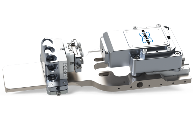
PICOINDENTER: Bruker Hysitron PI89
- Used for nanoindentation, tensile testing, pillar compression, cantilever bending, fracture, fatigue, dynamic testing, mechanical properties mapping
- Intrinsic displacement actuation and displacement control from <1nm to 150µm
- Load range from <1µN to 3.5N, and 78kHz
- 1 nm encoded linear stages provide greater repeatability during automated testing modes while increasing travel range
- The uniquely low-current design of the transducer minimizes thermal drift and provides unprecedented load and displacement sensitivity
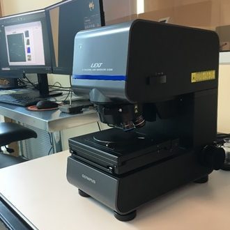
OLYMPUS LEXT OLS5000
- Non-contact, 3D, surface metrology at~10 nm resolution (z)
- Wide range of objectives: 5x, 10x, 20x (SLWD),50x (LWD), 100x
- Surface roughness, surface area, line profile,film thickness, step height measurements and more
- Automated report generation feature
- True, quantitative 3D imaging
- High aspect ratio structure measurements:measure surface features at up to 87° with respect to the light source
- Two imaging modes: 3D image + true color optical microscope image
WOOLLAM VARIABLE ANGLE SPECTROSCOPIC ELLIPSOMETER (VASE)
- Measurement of thickness of transparent thin films (i.e., optical coatings, photosensitive coatings
- Measurement of index of refraction and extinction coefficient
- Applicable to thin film thickness ranging from 1 monolayer to >1 micrometer
- Useful for single layer, and multilayer components
- Light source wavelength range: 190 – 2000 nm
- Xe Arc lamp and monochromator
- Angles: 70 – 75° for typical measurement
- Designed for planar samples
- Can hold wafers up to 4”
- Automated multi-spot data collection