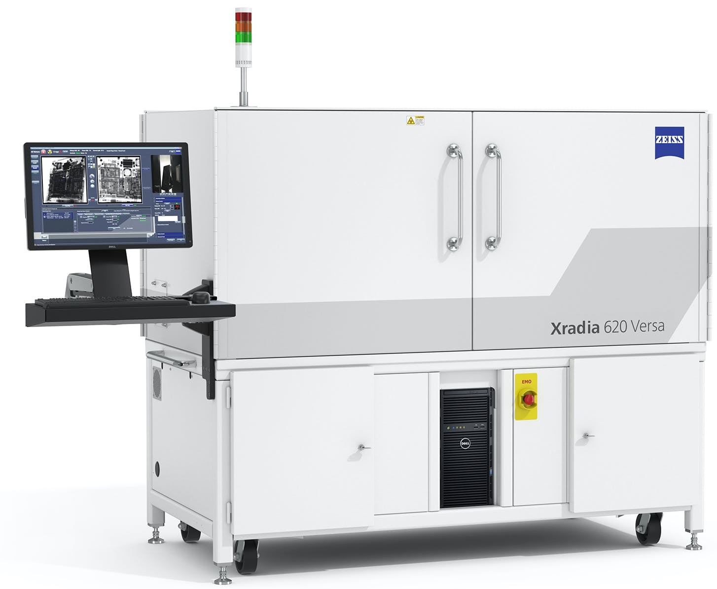
The X-ray Microscope provides non-destructive, 3D imaging of materials at up to 600 nm resolution
General Use and Application
-
- Crystallographic imaging modalities enabled by lab DCT
- Characterize material evolution over time (heat, cool, mechanical load)
- In-situ heating/cooling/tension/compression stage. Up to 5kN loads to materials.
- Large volume sample imaging enabled by Flat Panel Extension
- Tomographic Reconstruction software
- 3D visualization and segmentation software (Dragonfly Pro)
Click here to see the Nano-CT in operation!
For more information please contact:
Dr. Brian Van Devener (801-585-6162; b.van-devener@utah.edu)
Imaging Capabilities
- Deben CT5000-TEC 5kN in situ load/tensile stage. Cooling/heating from -20 C to +160 C
- High spatial resolution (600 nm)
- High resolution imaging at large working distances (RaaD)
- Flat panel extension (FPX) enables large volume imaging for large samples
- Versatile sample types and sizes. Stage travel range: x – 50 mm, y – 100 mm, z – 50 mm
- Lab DCT enables crystallographic imaging modalities
- DragonFly Pro Software for 3D imaging and reconstruction
- Wide Field imaging mode: 0.4x, 4x
- High resolution 40x detector kit
- 160kV, 25W microfocus xray source
| HOURLY RATES | ||
| Users | Daytime | Overnight M-F: 5pm - 8am Sat-Sun: All Day |
| On-Campus members | $60.00 | $30.00 |
| Off-Campus Academic | $92.40 | $46.20 |
| Industry | $120.00 | $60.00 |
| CONTACT US FOR RESERVATIONS: | |
| Dr. Randy Polson | Lab: 801-587-3108 Office: 801-587-0873 |
Specific Use and Application

Microscopy Solutions for Materials Science
- Characterize three-dimensional structure
- Observe failure mechanisms, degradation phenomena, and internal defects
- Investigate properties at multiple length scales
- Quantify microstructural evolution
- Perform in situ and 4D (time dependent) studies to understand the impact of heating, cooling, desiccation, wetting, tension, compression, imbibition, drainage and other simulated environmental studies
- Understand the 3D structure of fibers as well as pores and pore pathways in paper
- Observe the propagation of a crack inside your sample

Electronics and Semiconductors
- Perform structural and failure analysis for process development, yield improvement and construction analysis of advanced semiconductor packages, including 2.5/3D and fan-out packages
- Analyze printed circuit boards for reverse engineering and hardware security
- Non-destructively image across length scales from module to package to interconnect for submicron-resolution characterization of defects at speeds that can complement physical cross-sectioning
- Enable better understanding of defect locations and distributions by viewing unlimited virtual cross-section and plan-view images from all desired angles

Microscopy Solutions for Additive Manufacturing
- Detailed shape, size, and volume distribution analysis of particles in Additive Manufacturing (AM) powder bed to determine proper process parameters
- High-resolution, non-destructive imaging for microstructural analysis of AM parts
- 3D imaging for comparison with the nominal CAD representation
- Detection of unmelted particles, high-Z inclusions, and voids
- Surface roughness analysis of inner structures that cannot be accessed by other methods

Microscopy Solutions for Raw Materials
- Achieve automated mineralogy in 3D with little to no sample prep
- Perform multiscale pore structure and fluid flow analysis, directly measure fluid flow using in situ flow equipment
- Perform non-destructive scout scans and cut to ROI for buried structures in metamorphic rocks
- Analyze grain orientations in steel and other metals