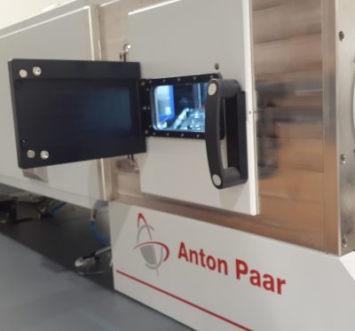
SAXSPOINT 5.0 SAXS/WAXS/GISAXS/RHEOSAXS LABORATORY BEAMLINE
- determining size and shape of monodisperse macromolecules
- measuring pore size
- nanoparticle size distribution
- distances of partially ordered materials
- general characterization of micro- to nanoscale structure of particle systems (i.e. average particle size, shapes, distribution, and surface-to-volume ratio
- samples can be solid, liquid or a mixture of both
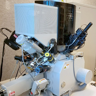
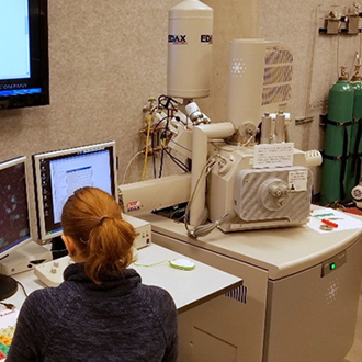
DUAL BEAM SEM/FIB: HELIOS NANOLAB 650
- High-resolution imaging <10 nm resolution for conductive materials
- Elemental contrast using backscatter electron imaging
- Low-voltage, low-current imaging of non-conductive samples
- Elemental mapping and semi-quantitative compositional analysis using energy dispersive spectroscopy (EDS)
- Automated particle morphology and elemental analysis using EDS
- Voltage contrast imaging
- Grain analysis (grain size, orientation and texture) using electron backscatter diffraction (EBSD)
- Automated particle morphology and elemental analysis using EDS
- Sectioning of thin specimen using ion beam
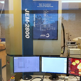
JEOL JEM 2800 SCANNING/TRANSMISSION ELECTRON MICROSCOPE (STEM)
- Sub nanometer high-resolution imaging for crystalline materials
- Elemental contrast imaging using STEM bright and dark field modes
- Nanoscale imaging of organic and biological samples in wet conditions with the use of the Protochips Poseidon wet cell
- Nanoscale imaging of samples under varying conditions of high temperature, high pressure and different reactive gases with the use of the Protochips atmospheric cell holder
- Nanoscale3D tomography imaging
- Crystal structure analysis from micron to nanometer scale using wide array of diffraction techniques - selected area (SAED), nano-beam (NBD), and convergent beam (CBD) diffraction
- Nanometer-scale and fast elemental mapping and compositional analysis using dual detector energy dispersive spectroscopy (EDS)
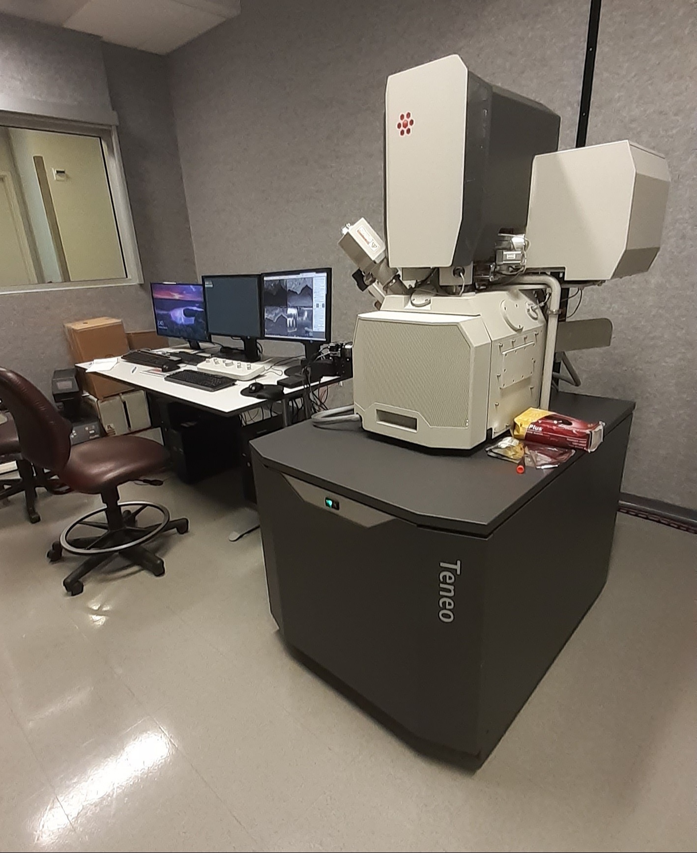
LOW-VOLTAGE SEM: FEI TENEO
- High-resolution imaging ~20 nm resolution for conductive and non-conductive materials
- Hight resolution imaging of non-conductive materials i.e., ceramics, polymers and biological samples at low voltages, without the aid of conductive coating
- Imaging of large (up to 100 cm diameter) samples without sectioning
- Elemental contrast using backscatter electron imaging
- Elemental mapping and semi-quantitative compositional analysis using energy dispersive spectroscopy (EDS)
- Grain analysis (grain size, orientation and texture) using electron backscatter diffraction (EBSD)
ENVIRONMENTAL SEM: QUANTA 600F
- High-resolution imaging ~20 nm resolution for conductive materials
- Imaging of large (up to 6 inch diameter) samples without sectioning
- Elemental contrast using backscatter electron imaging
- Imaging of non-conductive materials i.e., ceramics, polymers and biological samples, without the aid of conductive coating
- Imaging of wet samples using environmental mode
- Voltage contrast imaging
- Elemental mapping and semi-quantitative compositional analysis using energy dispersive spectroscopy (EDS)
- Automated particle morphology and elemental analysis using EDS
- Grain analysis (grain size, orientation and texture) using electron backscatter diffraction (EBSD)