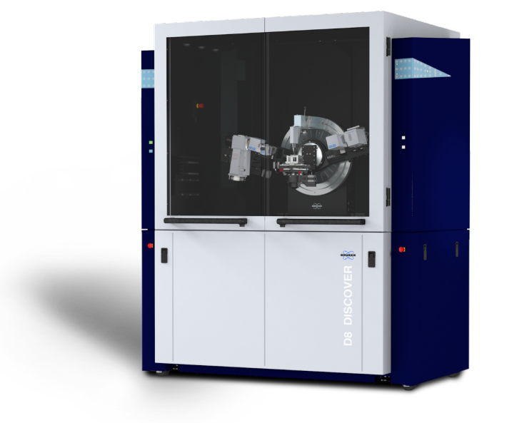
BRUKER DISCOVER D8 HIGH RESOLUTION XRD WITH HEATED STAGE
- Phase identification and quantification, structure determination and refinement, micro-strain and crystallite size analysis.
- X-Ray reflectometry, Grazing Incidence Diffraction (GID), In-Plane Diffraction, High-resolution XRD, GISAXS, GI-Stress analysis, crystal orientation analysis.
- Residual stress analysis, texture and pole figures.
- Total scattering analysis: Bragg Diffraction, Pair-Distribution Function (PDF)
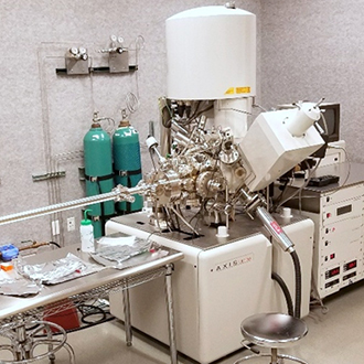
X-RAY, AUGER, ULTRAVIOLET PHOTOELECTRON SPECTROSCOPY (XPS),(AES),(UPS): KRATOS AXIS ULTRA
- Quantitative chemical analysis of the top 10 nm surface layer
- Identification of bonding and oxidation state of elements on the surface
- Overlayer thickness measurement up to ~10 nm
- Depth profiling of up to ~100 nm using Ar+ ion sputtering
- Fermi-level and work function measurement via ultraviolet photoelectron spectroscopy (UPS) with He(I) and He(II) sources
- Scanning electron and scanning auger microscopy ~15 μm resolution
- Chemical analysis of the top monolayer using ion scattering spectroscopy (ISS) with He ion source
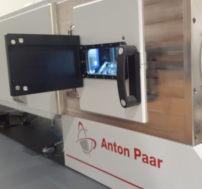
SAXSPOINT 5.0 SAXS/WAXS/GISAXS/RHEOSAXS LABORATORY BEAMLINE
- determining size and shape of monodisperse macromolecules
- measuring pore size
- nanoparticle size distribution
- distances of partially ordered materials
- general characterization of micro- to nanoscale structure of particle systems (i.e. average particle size, shapes, distribution, and surface-to-volume ratio
- samples can be solid, liquid or a mixture of both
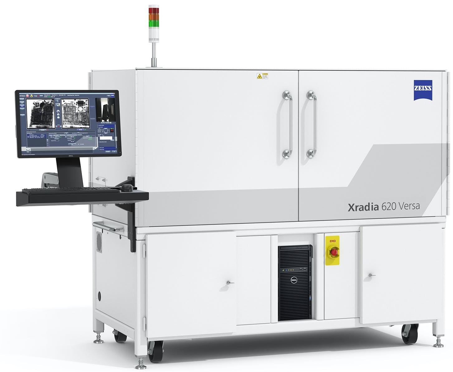
ZEISS XRADIA VERSA 620 3D X-RAY MICROSCOPE/NANO-CT
- Crystallographic imaging modalities enabled by lab DCT
- Characterize material evolution over time (heat, cool, mechanical load)
- In-situ heating/cooling/tension/compression stage. Up to 5kN loads to materials.
- Large volume sample imaging enabled by Flat Panel Extension
- Tomographic Reconstruction software
- 3D visualization and segmentation software (Dragonfly Pro)
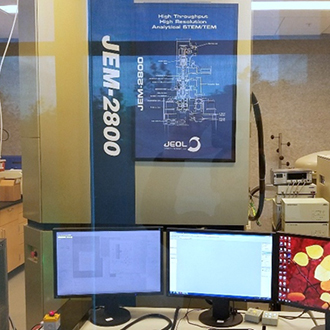
NANOSCALE EDS JEOL JEM 2800 S/TEM
- Sub nanometer high-resolution imaging for crystalline materials
- Elemental contrast imaging using STEM bright and dark field modes
- Nanoscale imaging of organic and biological samples in wet conditions with the use of the Protochips Poseidon wet cell
- Nanoscale imaging of samples under varying conditions of high temperature, high pressure and different reactive gases with the use of the Protochips atmospheric cell holder
- Nanoscale3D tomography imaging
- Crystal structure analysis from micron to nanometer scale using wide array of diffraction techniques - selected area (SAED), nano-beam (NBD), and convergent beam (CBD) diffraction
- Nanometer-scale and fast elemental mapping and compositional analysis using dual detector energy dispersive spectroscopy (EDS)
MICRON-SCALE EDS QUANTA 600F ENVIRONMENTAL SEM
- High-resolution imaging ~20 nm resolution for conductive materials
- Imaging of large (up to 6 inch diameter) samples without sectioning
- Elemental contrast using backscatter electron imaging
- Imaging of non-conductive materials i.e., ceramics, polymers and biological samples, without the aid of conductive coating
- Imaging of wet samples using environmental mode
- Voltage contrast imaging
- Elemental mapping and semi-quantitative compositional analysis using energy dispersive spectroscopy (EDS)
- Automated particle morphology and elemental analysis using EDS
- Grain analysis (grain size, orientation and texture) using electron backscatter diffraction (EBSD)
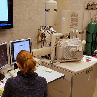
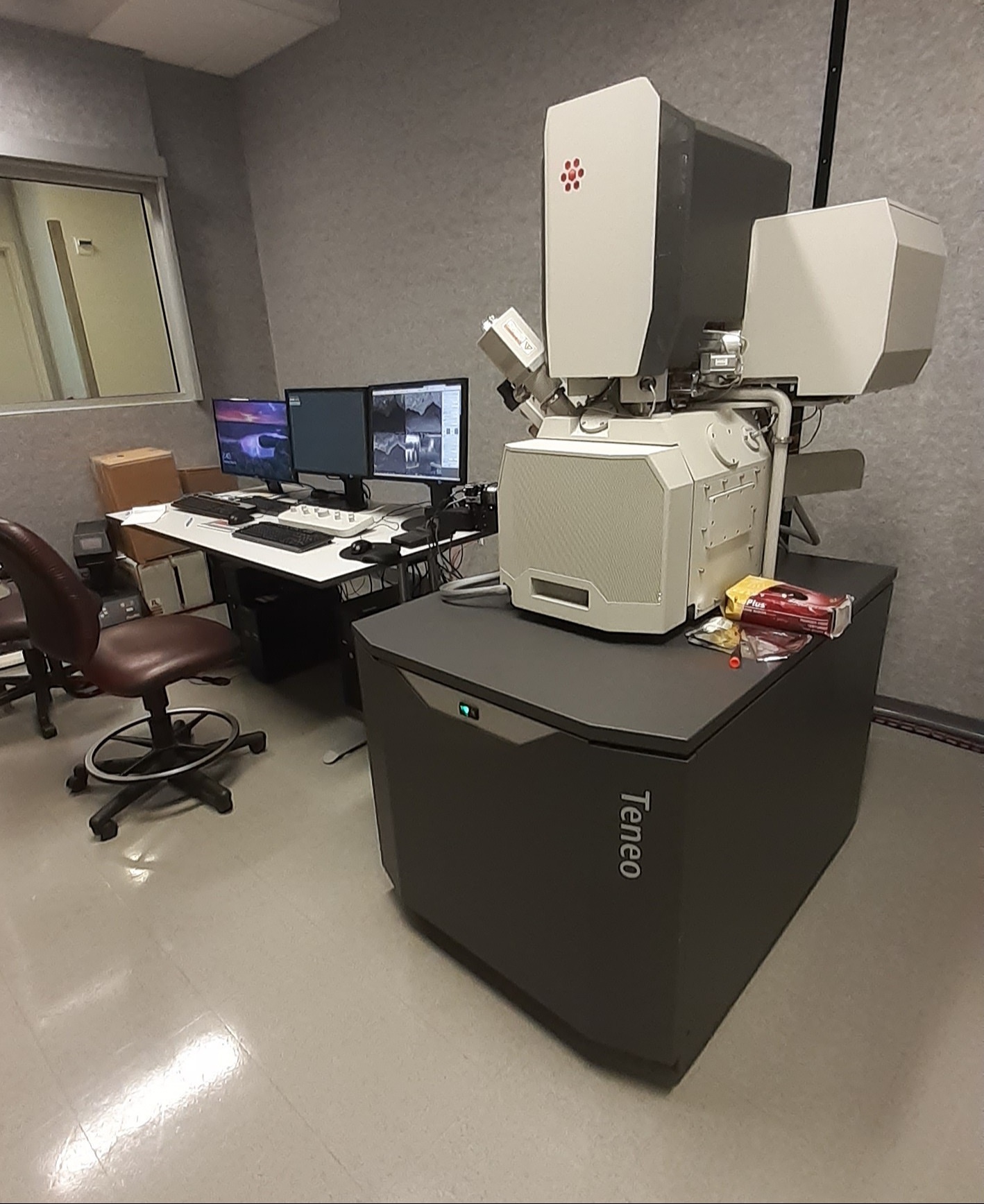
MICRON-SCALE EDS FEI TENEO LOW-VOLTAGE SEM
- High-resolution imaging ~20 nm resolution for conductive and non-conductive materials
- Hight resolution imaging of non-conductive materials i.e., ceramics, polymers and biological samples at low voltages, without the aid of conductive coating
- Imaging of large (up to 100 cm diameter) samples without sectioning
- Elemental contrast using backscatter electron imaging
- Elemental mapping and semi-quantitative compositional analysis using energy dispersive spectroscopy (EDS)
- Grain analysis (grain size, orientation and texture) using electron backscatter diffraction (EBSD)
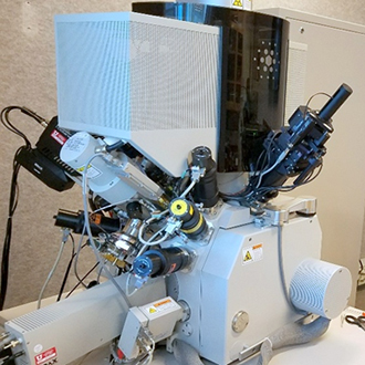
MICRON-SCALE EDS HELIOS NANOLAB 650 DUAL BEAM SEM/FIB
- High-resolution imaging <10 nm resolution for conductive materials
- Elemental contrast using backscatter electron imaging
- Low-voltage, low-current imaging of non-conductive samples
- Elemental mapping and semi-quantitative compositional analysis using energy dispersive spectroscopy (EDS)
- Automated particle morphology and elemental analysis using EDS
- Voltage contrast imaging
- Grain analysis (grain size, orientation and texture) using electron backscatter diffraction (EBSD)
- Automated particle morphology and elemental analysis using EDS
- Sectioning of thin specimen using ion beam
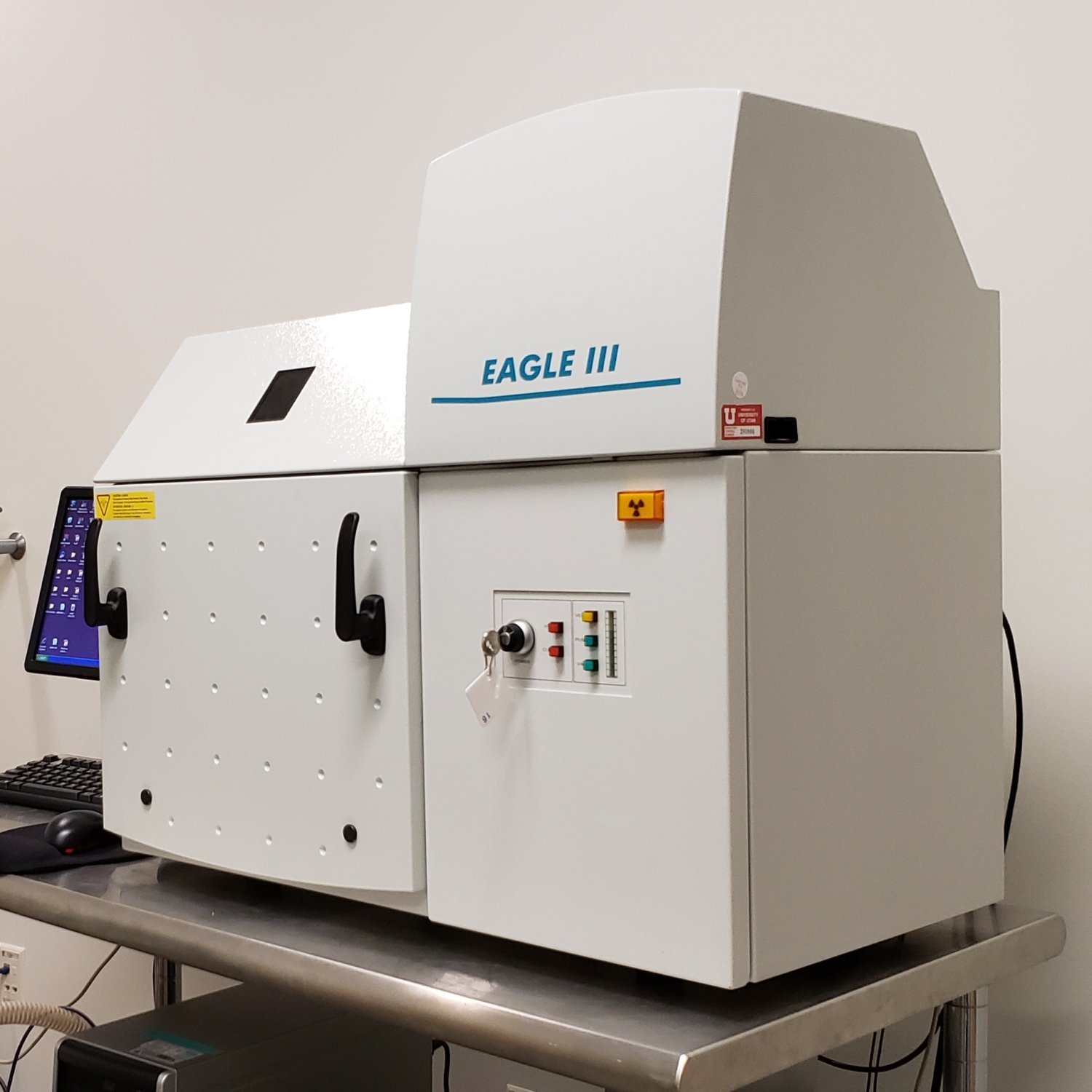
MICRON-MILLIMETER SCALE EDS EAGLE III MICROSPOT X-RAY FLUORESCENCE SPECTROMETER (XRF)
- Capable of detecting elements rom Na to U
- 0.1 mm spatial resolution
- Automated stage movement for elemental mapping
- Up to 10 cm x 10 cm area of sample mapping
